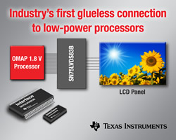
TI 公司的SN75LVDS83B是FlatLink發(fā)送器,包括有四個7位并行負(fù)載串行輸出的移為寄存器,7X時鐘合成器,以及5個LVDS線路驅(qū)動器,可以把28位單端LV
TTL數(shù)據(jù)同步地在5個平衡對導(dǎo)體上發(fā)送,由兼任的接收器接收如SN75LVDS82和集成了LVDS接收器的LCD屏.數(shù)據(jù)傳輸速率高達(dá)135M像素/秒,像素時腫范圍從10MHz到135MHz,工作電壓3.3V,75MHz時的功耗為170mW,可用于LCD屏驅(qū)動器,UMPC和筆記本電腦以及數(shù)碼相框等.本文介紹了SN75LVDS83B的主要特性,方框圖以及多種連接到LCD屏的應(yīng)用電路和SN75LVDS83B評估模塊電路圖.
The SN75LVDS83B FlatLink™ transmitter contains four 7-bit parallel-load serial-out shift registers, a 7X clock synthesizer, and five Low-Voltage Differential Signaling (LVDS) line drivers in a single integrated circuit. These functions allow 28 bits of single-ended LV
TTL data to be synchronously transmitted over five balanced-pair conductors for receipt by a compatible receiver, such as the SN75LVDS82 and LCD panels with integrated LVDS receiver.
When transmitting, data bits D0 through D27 are each loaded into registers upon the edge of the input clock signal (CLKIN). The rising or falling edge of the clock can be selected via the clock select (CLKSEL) pin. The frequency of CLKIN is multiplied seven times, and then used to unload the data registers in 7-bit slices and serially. The four serial streams and a phase-locked clock (CLKOUT) are then output to LVDS output drivers. The frequency of CLKOUT is the same as the input clock, CLKIN.
The SN75LVDS83B requires no external components and little or no control. The data bus appears the same at the input to the transmitter and output of the receiver with the data transmission transparent to the user(s). The only user intervention is selecting a clock rising edge by inputting a high level to CLKSEL or a falling edge with a low-level input, and the possible use of the Shutdown/Clear (SHTDN). SHTDN is an active-low input to inhibit the clock, and shut off the LVDS output drivers for lower power consumption. A low-level on this signal clears all internal registers to a low-level.
The SN75LVDS83B is characterized for operation over ambient air temperatures of -10℃ to 70℃.
SN75LVDS83B主要特性:
LVDS Display Serdes Interfaces Directly to LCD Display Panels with Integrated LVDS
Package Options: 4.5mm x 7mm BGA, and 8.1mm x 14mm TSSOP
1.8V up to 3.3V Tolerant Data Inputs to Connect Directly to Low-Power, Low-Voltage Application and Graphic Processors
Transfer Rate up to 135Mpps (Mega Pixel Per Second); Pixel Clock Frequency Range 10MHz to 135MHz
Suited for Display Resolutions Ranging From HVGA up to HD With Low EMI
Operates From a Single 3.3V Supply and 170mW (typ.) at 75MHz
28 Data Channels Plus Clock In Low-Voltage
TTL to 4 Data Channels Plus Clock Out Low-Voltage Differential
Consumes Less Than 1mW When Disabled
Selectable Rising or Falling Clock Edge Triggered Inputs
ESD: 5kV HBM
Support Spread Spectrum Clocking (SSC)
Compatible with all OMAP™2x, OMAP™3x, and DaVinci™ Application Processors
SN75LVDS83B應(yīng)用:
LCD Display Panel Driver
UMPC and Netbook PC
Digital Picture Frame
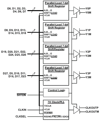
圖1.SN75LVDS83B功能方框圖
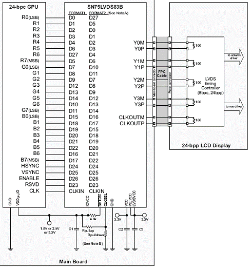
圖2.SN75LVDS83B在24位彩色主機(jī)連接到24位LCD屏的應(yīng)用
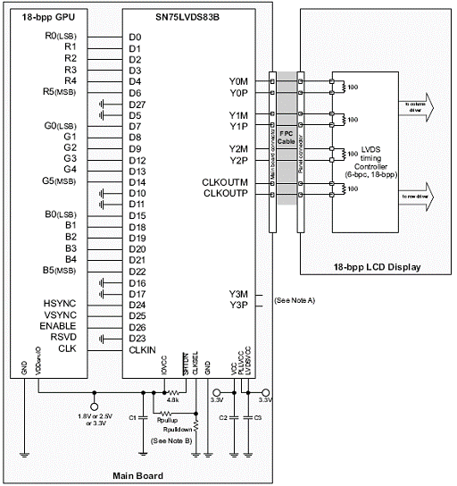
圖3.SN75LVDS83B在18位彩色主機(jī)連接到18位LCD屏的應(yīng)用
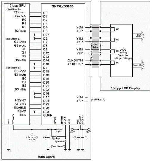
圖4.SN75LVDS83B在12位彩色主機(jī)連接到18位LCD屏的應(yīng)用
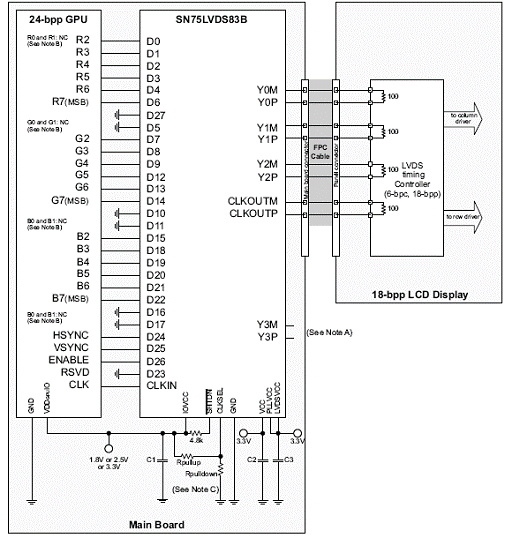
圖5.SN75LVDS83B在24位彩色主機(jī)連接到18位LCD屏的應(yīng)用
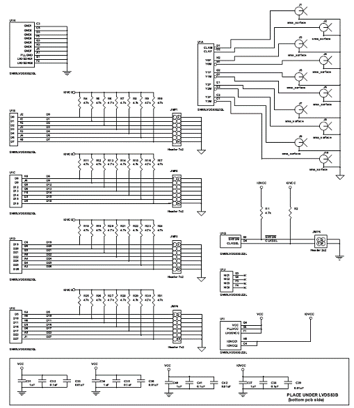
圖6.SN75LVDS83B評估模塊電路圖