用有源鉗位正激轉(zhuǎn)換器閉環(huán)
2019-11-14 15:01:08 安森美

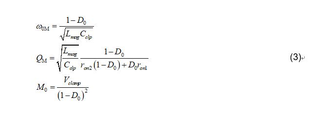


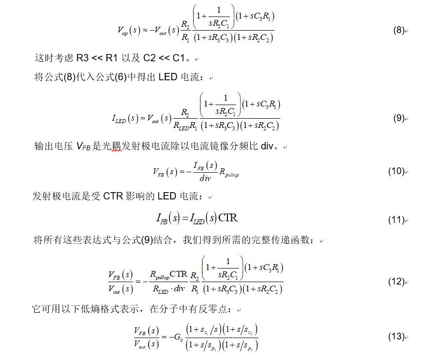
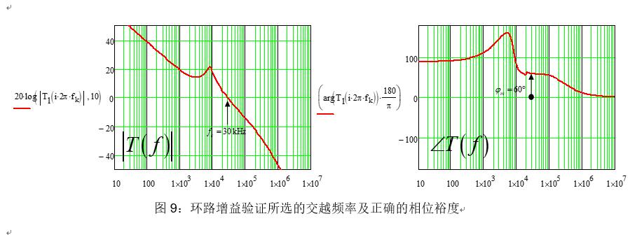
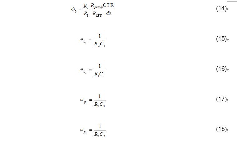 現(xiàn)在我們已有補(bǔ)償器傳遞函數(shù),我們需要一種方法來(lái)調(diào)整交越點(diǎn)上的期望增益或衰減。可以通過(guò)選擇正確的R2值,同時(shí)需要考慮由設(shè)計(jì)固定的或制造商強(qiáng)加的其他器件值(例如,電路中的Rpullup)。公式(12)的幅值由下式確定:
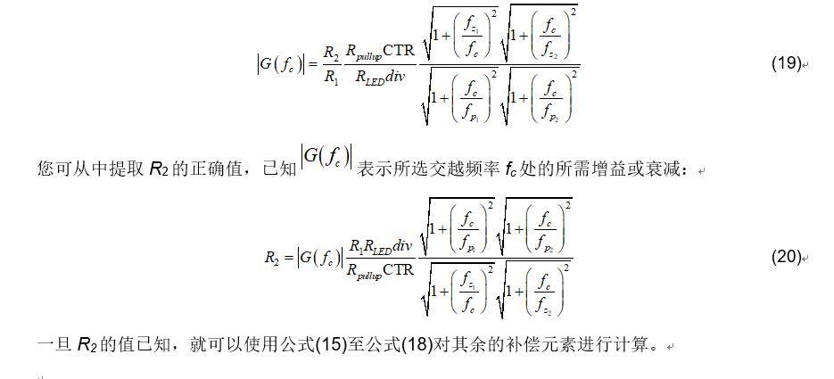


EETOP 官方微信

創(chuàng)芯大講堂 在線教育

半導(dǎo)體創(chuàng)芯網(wǎng) 快訊
相關(guān)文章